- 您现在的位置:买卖IC网 > Sheet目录3879 > PIC18F65J11-I/PT (Microchip Technology)IC PIC MCU FLASH 16KX16 64TQFP
2010 Microchip Technology Inc.
DS39774D-page 107
PIC18F85J11 FAMILY
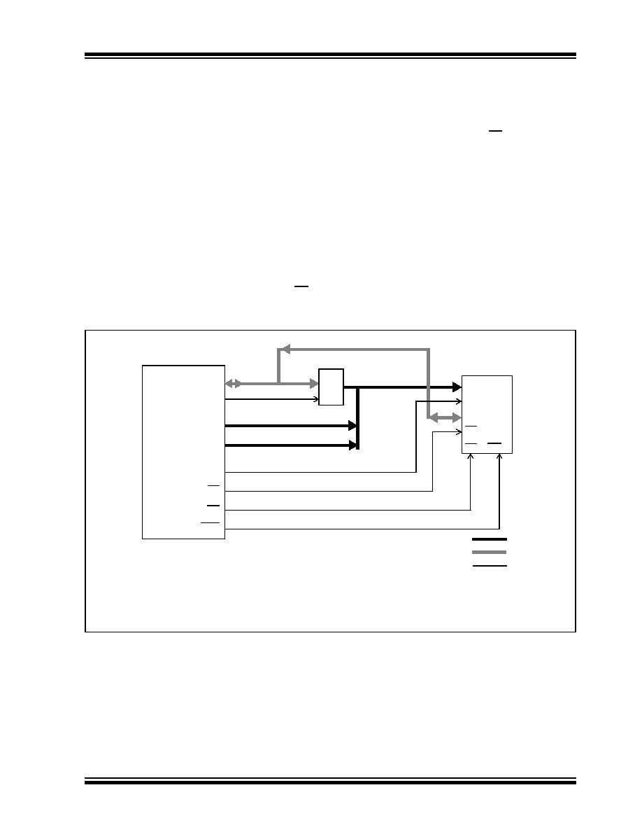
8.7
8-Bit Data Width Mode
In 8-Bit Data Width mode, the external memory bus
operates only in Multiplexed mode; that is, data shares
the 8 Least Significant bits of the address bus.
Figure 8-6 shows an example of 8-Bit Multiplexed
mode for 80-pin devices. This mode is used for a single
8-bit memory connected for 16-bit operation. The
instructions will be fetched as two 8-bit bytes on a
shared data/address bus. The two bytes are sequen-
tially fetched within one instruction cycle (TCY).
Therefore, the designer must choose external memory
devices according to timing calculations based on
1/2 TCY (2 times the instruction rate). For proper mem-
ory speed selection, glue logic propagation delay times
must be considered, along with setup and hold times.
The Address Latch Enable (ALE) pin indicates that the
address bits, AD<15:0>, are available on the external
memory interface bus. The Output Enable signal (OE)
will enable one byte of program memory for a portion of
the instruction cycle, then BA0 will change and the
second byte will be enabled to form the 16-bit instruc-
tion word. The Least Significant bit of the address, BA0,
must be connected to the memory devices in this
mode. The Chip Enable signal (CE) is active at any
time that the microcontroller accesses external
memory, whether reading or writing. It is inactive
(asserted high) whenever the device is in Sleep mode.
This generally includes basic EPROM and Flash
devices. It allows table writes to byte-wide external
memories.
During a TBLWT instruction cycle, the TABLAT data is
presented on the upper and lower bytes of the
AD<15:0> bus. The appropriate level of the BA0 control
line is strobed on the LSb of the TBLPTR.
FIGURE 8-6:
8-BIT MULTIPLEXED MODE EXAMPLE
AD<7:0>
A<19:16>(1)
ALE
D<15:8>
373
A<19:0>
A<x:1>
D<7:0>
OE
WR(2)
CE
Note 1:
The upper order address bits are only used 20-bit address width. The upper AD byte is used for all
address widths except 8-bit.
2:
This signal only applies to table writes. See Section 7.1 “Table Reads and Table Writes”.
WRL
D<7:0>
PIC18F85J11
AD<15:8>(1)
Address Bus
Data Bus
Control Lines
CE
A0
BA0
发布紧急采购,3分钟左右您将得到回复。
相关PDF资料
PIC18F2439-E/SO
IC PIC MCU FLASH 6KX16 28SOIC
PIC16LF1938-I/SS
IC MCU 8BIT FLASH 28SSOP
PIC16C621A-20/SO
IC MCU OTP 1KX14 COMP 18SOIC
PIC18F23K22-I/SO
IC PIC MCU 8KB FLASH 28SOIC
PIC18LF2331-I/MM
IC MCU FLASH 4KX16 28QFN
PIC16F639-I/P
IC MCU FLASH 2KX14 20DIP
PIC18F25K20-I/SS
IC PIC MCU FLASH 16KX16 28SSOP
PIC16C58B-04/P
IC MCU OTP 2KX12 18DIP
相关代理商/技术参数
PIC18F65J11T-I/PT
功能描述:8位微控制器 -MCU 32KB Flash 2048bytes-RAM 51I/O RoHS:否 制造商:Silicon Labs 核心:8051 处理器系列:C8051F39x 数据总线宽度:8 bit 最大时钟频率:50 MHz 程序存储器大小:16 KB 数据 RAM 大小:1 KB 片上 ADC:Yes 工作电源电压:1.8 V to 3.6 V 工作温度范围:- 40 C to + 105 C 封装 / 箱体:QFN-20 安装风格:SMD/SMT
PIC18F65J15-I/PT
功能描述:8位微控制器 -MCU 32 KB FL 2KB RAM RoHS:否 制造商:Silicon Labs 核心:8051 处理器系列:C8051F39x 数据总线宽度:8 bit 最大时钟频率:50 MHz 程序存储器大小:16 KB 数据 RAM 大小:1 KB 片上 ADC:Yes 工作电源电压:1.8 V to 3.6 V 工作温度范围:- 40 C to + 105 C 封装 / 箱体:QFN-20 安装风格:SMD/SMT
PIC18F65J15T-I/PT
功能描述:8位微控制器 -MCU 32 KB FL 2KB RAM RoHS:否 制造商:Silicon Labs 核心:8051 处理器系列:C8051F39x 数据总线宽度:8 bit 最大时钟频率:50 MHz 程序存储器大小:16 KB 数据 RAM 大小:1 KB 片上 ADC:Yes 工作电源电压:1.8 V to 3.6 V 工作温度范围:- 40 C to + 105 C 封装 / 箱体:QFN-20 安装风格:SMD/SMT
PIC18F65J50-I/PT
功能描述:8位微控制器 -MCU 32KB FLSH 3936Bs RAM USB 2.0 nanoWatt RoHS:否 制造商:Silicon Labs 核心:8051 处理器系列:C8051F39x 数据总线宽度:8 bit 最大时钟频率:50 MHz 程序存储器大小:16 KB 数据 RAM 大小:1 KB 片上 ADC:Yes 工作电源电压:1.8 V to 3.6 V 工作温度范围:- 40 C to + 105 C 封装 / 箱体:QFN-20 安装风格:SMD/SMT
PIC18F65J50T-I/PT
功能描述:8位微控制器 -MCU 32KB FLSH 3936Bs RAM USB 2.0 nanoWatt RoHS:否 制造商:Silicon Labs 核心:8051 处理器系列:C8051F39x 数据总线宽度:8 bit 最大时钟频率:50 MHz 程序存储器大小:16 KB 数据 RAM 大小:1 KB 片上 ADC:Yes 工作电源电压:1.8 V to 3.6 V 工作温度范围:- 40 C to + 105 C 封装 / 箱体:QFN-20 安装风格:SMD/SMT
PIC18F65J90-I/PT
功能描述:8位微控制器 -MCU 32KB FL 2048b RAM 51I/O 8b Fam RoHS:否 制造商:Silicon Labs 核心:8051 处理器系列:C8051F39x 数据总线宽度:8 bit 最大时钟频率:50 MHz 程序存储器大小:16 KB 数据 RAM 大小:1 KB 片上 ADC:Yes 工作电源电压:1.8 V to 3.6 V 工作温度范围:- 40 C to + 105 C 封装 / 箱体:QFN-20 安装风格:SMD/SMT
PIC18F65J90-I/PT
制造商:Microchip Technology Inc 功能描述:IC MCU 8BIT 32K FLASH SMD TQFP64
PIC18F65J90T-I/PT
功能描述:8位微控制器 -MCU 32KB Flash 2048bytes-RAM 51I/O RoHS:否 制造商:Silicon Labs 核心:8051 处理器系列:C8051F39x 数据总线宽度:8 bit 最大时钟频率:50 MHz 程序存储器大小:16 KB 数据 RAM 大小:1 KB 片上 ADC:Yes 工作电源电压:1.8 V to 3.6 V 工作温度范围:- 40 C to + 105 C 封装 / 箱体:QFN-20 安装风格:SMD/SMT